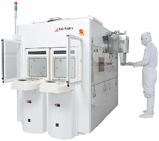
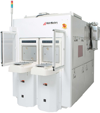
MRS-300
多波長高分解能ラマン測定装置 (MRS: Multiwavelength Raman Spectroscopy)
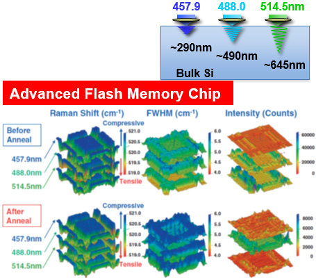
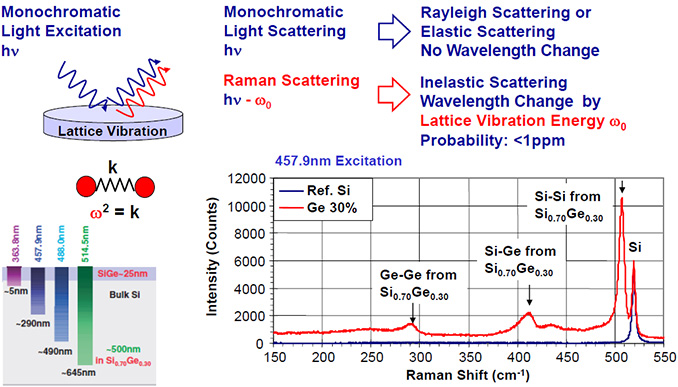
Multi-wavelength Raman Spectroscopy allows depth profiling of lattice stress characteristics, dopant activation, implant species concentration, and other process parameters with great measurement stability. This technology is being applied to new challenges in Si stress characterization in advanced devices and TSV structures. Ge content uniformity and SiGe layer thickness monitoring of SiGe/Si has become an exciting application in the last few years.
Multiwavelength Raman Spectroscopy
Multi-wavelength Raman Spectroscopy
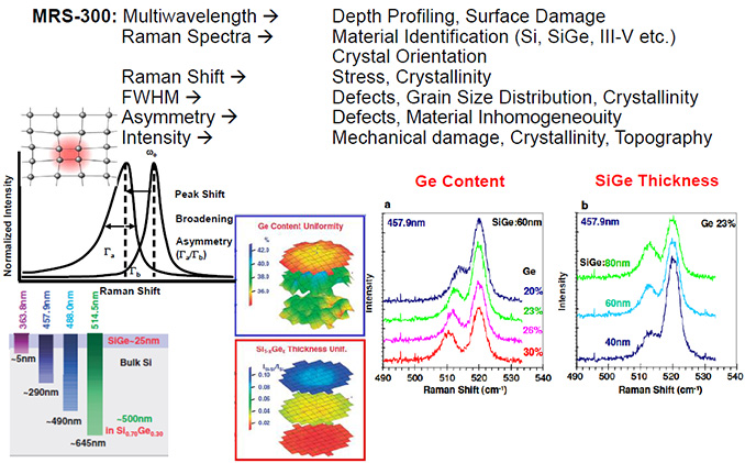
JJAP論文
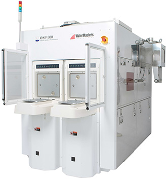
OSP-300
Optical Surface Profilometry
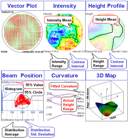
Optical Surface Profilometry is an accurate direct measurement technology for mapping the wafer surface, showing local maxima, minima and shape changes due to global and local distortion with process sequence. Often this data can be correlated to stress changes, pattern overlay and wafer breakage problems along process steps.
MPL-300
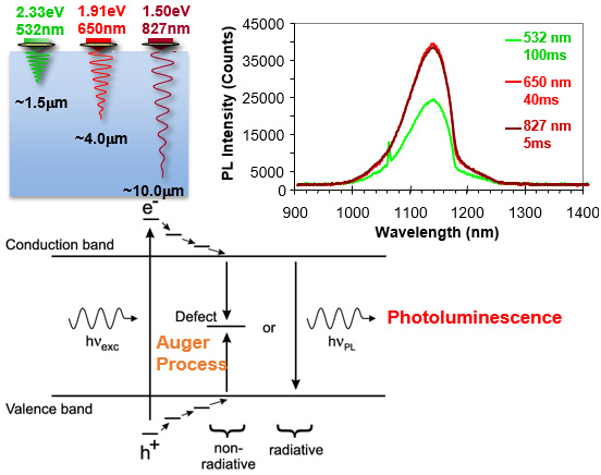
Multiwavelength Photoluminescence
Multiwavelength Photoluminescence Spectroscopy: The most direct way to measure band-gap energies, dopant activation, electrically active defects, plasma induced damage (PID), dielectrics/Si interface quality, metal contamination which affect minority carrier lifetime and electron mobility characteristics of the semiconductor.

